
MIT scientists have developed a cutting-edge technology to grow layers of 2D transition metal dichcogenide (TMD) material on an entirely produced silicon chip. Scientists have developed a low-temperature growth process for 2D semiconductors.
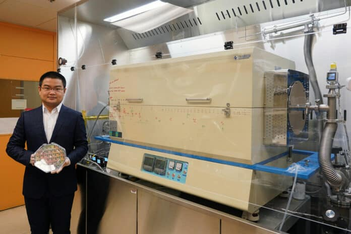
According to scientists, new technology reduces the time it takes to grow. It can create a uniform layer of TMD material in 30 minutes over 8-inch wafers.
This method is better for commercial applications where an 8-inch layer is essential. According to the study, inventors mainly work on molybdenum disulfide because it is very flexible, transparent, and exhibits electronic and photonic properties, all properties of semiconductors. One layer of molybdenum sandwiched between two sulphur atoms.
Two layers of organic chemical compounds contain molybdenum hexcarbonyl and diethylene sulphur. The vaporizing and heating reaction chambers create smaller molecules that decompose into smaller molecules. They link through chains of molybdenum disulfide on the surface that decompose up to a maximum temperature of 550 degrees Celsius, with the silicon circuit star degrading after 400 degrees Celsius. Molybdenum and sulphur control temperatures below 400 degrees Celsius.
They inserted silicon wafer vertically opposite to horizontally where the low temperature are of furnace, because they not need too high temperature because of high heat damage the wafers. Horizontally surface they collide with vertical chip of Molybdenum and sulfur gas molecule they enhance circular motion in homogeneity material.
For yielding a more uniform layer, this method was much faster than the MOCVD process. MOCVD growth processes take a whole day. They have homogeneity and quality throughout an 8-inch silicon wafer using MIT Nano technology for commercial applications.